厂商 :英尚国际微电子
广东 深圳- 主营产品:
- 集成电路
- 电子元器件
- SRAM

品牌:Netsol
型号:S7T3209T4M(索取规格书请联系137-5119-2970)www.sramsun.com
1Mx36 & 2Mx18 & 4Mx9 - Bit Quadruple-II+ Burst Length of 4 SRAM w/ ODT
Features General Description
|
?1.8V+0.1V/-0.1V Power Supply. ?DLL circuitry for wide output data valid window and future fre- quency scaling. ?I/O Supply Voltage 1.5V+0.1V/-0.1V for 1.5V I/O, 1.8V+0.1V/ -0.1V for 1.8V I/O. ?Separate independent read and write data ports with concurrent read and write operation ?HSTL I/O ?Full data coherency, providing most current data. ?Synchronous pipeline read with self timed late write ?Read latency : 2 clock cycles. ?Registered address, control and data input/output. ?DDR (Double Data Rate) Interface on read and write ports. ?Fixed 4-bit burst for both read and write operation. ?Clock-stop supports to reduce current. ?Two input clocks (K and K) for accurate DDR timing at clock rising edges only. ?Two echo clocks (CQ and CQ) to enhance output data traceability. ?Data Valid pin(QVLD) supported ?On die termination (ODT) supported for data input, K, K and BWx. ?Single address bus. ?Byte write (x9, x18, x36) function. ?Separate read/write control pin (R and W) ?Simple depth expansion with no data contention. ?Programmable output impedance(ZQ). ?JTAG 1149.1 compatible test access port. ?165FBGA(11x15 ball array FBGA) with body size of 13x15mm |
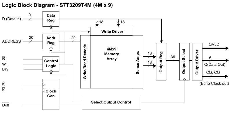
The S7T3236T4M, S7T3218T4M and S7T3209T4M are 37,748,736-bits Quadruple Synchronous Pipelined Burst SRAMs. They are organized as 1,048,576 words by 36bits for S7T3236T4M, 2,097,152 words by 18bits for S7T3218T4M and 4,194,304 words by 9bits for S7T3209T4M. The Quadruple operation is possible by supporting DDR read and write operations through separate data output and input ports with the same cycle. Memory bandwidth is maximized as data can be transferred into and out of SRAM on every rising edge of K and K. And totally independent read and write ports eliminate the need for high speed bus turn around. Address for read and write are latched on alternate rising edges of the input clock K. Data inputs and outputs, and all control signals are synchronized to the input clock (K or K). Read data are referenced to echo clock (CQ or CQ) outputs. The S7T3236T4M, S7T3218T4M and S7T3209T4M support On Die Termination (ODT) for data input, input clock (K, K) and BWx. On Die Termination can reduce the number of resistor elements and complex wiring on the system board. Accordingly, the system design can be simpler and cost effective. Common address bus is used to access address both for read and write operations. The internal burst counter is fixed to 4-bit sequential for both read and write operations requiring two full clock bus cycles. Any request that attempts to interrupt a burst opera- tion in progress is ignored. Synchronous pipeline read and late write enable high speed operations. Simple depth expansion is accomplished by using R and W for port selection. Byte write operation is supported with BW0 and BW1 (BW2 and BW3) pins for x18 (x36) device and only BW pin for x9 device
|
Key Parameters
|
Part Number |
Org. |
Freq. (MHz) |
Cycle Time (ns) |
Access Time (ns) |
RoHS |
|
S7T3236T4M-E(F)C(I)45 |
x36 |
450 |
2.2 |
0.45 |
Ο |
|
S7T3236T4M-E(F)C(I)40 |
400 |
2.5 |
0.45 |
Ο |
|
|
S7T3218T4M-E(F)C(I)45 |
x18 |
450 |
2.2 |
0.45 |
Ο |
|
S7T3218T4M-E(F)C(I)40 |
400 |
2.5 |
0.45 |
Ο |
|
|
S7T3209T4M-E(F)C(I)45 |
x9 |
450 |
2.2 |
0.45 |
Ο |
|
S7T3209T4M-E(F)C(I)40 |
400 |
2.5 |
0.45 |
Ο |


