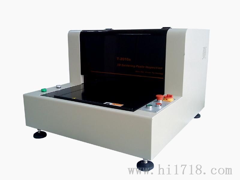
厂商 :深圳市泰金检测设备有限公司
广东 深圳- 主营产品:
- 锡膏测厚仪
- 链条油
- 测温仪

产品特征:◆可编程结构光栅 (PSLM), 实现了对光栅的软件调控。
◆同步漫反射专利技术消除阴影的影响。
◆支持460x350mm的PCB检测。
◆高桢数130万像素工业相机,精密级的丝杆导轨保证机械精度。
◆精确的测量体积,面积,高度,XY偏移,桥接等项目。
◆全板自动检测,自动路径优化。
◆对于有缺陷的锡膏,快速的进行检查及自动分类。
◆6~8次采样,可靠性,高精度的检测结果。
◆设备重复性精度<<10% (6 sigma)
<<10%?(6?sigma)
<<10% (6 sigma)
<<10%?(6?sigma)
◆自动消除板弯影响。
◆功能强大的过程控制软件(SPC)。
◆手工Teach功能应对无Gerber文件时的检测。
◆Gerber文件导入编程。
◆五分钟编程和一键式操作。
Product Features:
◆The use of PSLM combined with the PMP to achieve 100% high-precision solder
paste 3D measurement in SMT production line.
◆Using PSLM technology, changed the traditional way of generating 3D Struct
Light, the traditional glass grating moire (Moiré) required mechanically driven by a
piezoelectric motor (PZT). By using PSLM, no need glass grating and mechanical
parts any more. The elimination of the mechanical drive and moving parts, greatly
improving the ease of use and avoid mechanical wear and reduce maintenance
costs.
◆By using the Stop & Catch methods combined with multiple image acquisition,
realize highly repeatable 3D results on the solder paste measurement. Unlike
conventional scanning and it is just take one image on the solder paste a scan
sampling. Multiple image acquisition greatly enhanced the accuracy and reliable
test results.
◆Patented DL technology achieves full light spectrum detect ability. It is perfect
solution to solve the shadow effect and reduce noise interference during 3D
measurement.
◆Gerber data conversion and import, achieve automatic detection of the entire
board. Manual “Teach” function realize user-friendly programming and test job
generation in case of no Gerber data situation.
◆Friendly and simple user interface, five minutes of programming and one key
operation.
◆The maximum detectable height increased from the traditional ± 350um to
±1200um, not only can detect solder paste, also applies to the detection of
opaque objects such as red glue and black epoxy and other none transparent
object.
◆Powerful “Statistical Process Control (SPC)”, provide a plenty of tools, user-
friendly real-time monitoring, reduce defects caused by poor solder paste printing
and improve final product quality.
◆Fit up to 450 x 350mm PCB, Application range like: computer accessories, LCD TV,
audio-visual products, automotive electronics, medical electronics, etc.
|
Measurement Principle |
3D white light PSLM PMP |
|
Check the project |
Volume, area, height, position, shape, XY |
|
Bad type |
More / less tin, solder paste stencil, sharp pull, bridging, offset, special-shaped, dirt etc. |
|
FOV size |
25 * 20 mm |
|
Accuracy |
XY: 10 um, height: 1 um |
|
Repeatability |
Height: < 1um (4 sigma), volume: < 1% (5 sigma)<> |
|
Test speed |
<2.5 second /FOV |
|
Mark-point detection time |
1 second/1 pc |
|
Max Measurement Height |
+/-350 um, (+/- 1200 um, option) |
|
PCB maximum bending |
+/- 5 mm |
|
Min pad spacing |
100 um |
|
Min test size |
Rectangle: 150 um, Circle: 200 um |
|
Max PCB size |
460 * 350 mm |
|
Engineering Statistics |
Histogram; Xbar-R Chart; Xbar-S Chart; CP&CPK; %Gage Repeatability data; SPI daily/weekly/monthly reports |
|
Read position detection |
Gerber Format(274x,274d),Teach |
|
OS |
Windows XP professional or Windows 7 professional |
|
Dimension and weight |
810 * 930*530 mm, 125 kg |

