


厂商 :深圳创信电子科技有限公司
广东 深圳- 主营产品:
- 电子元器件
- 放大器IC
- 存储器
联系电话 :18926047716
商品详细描述
General Description
The RTL8198-GR is an integrated System-on-a-Chip (SoC) Application Specific Integrated Circuit (ASIC) that implements a L2 switch, L3 routing, and L4 NAT functions. An RLX5281 CPU is embedded and the clock rate can be 500MHz~620MHz. To improve computational performance, a 16-Kbyte I-Cache, 8-Kbyte D-Cache, 40-K I-MEM, and 8-Kbyte D-MEM are provided. A standard 5-signal P1149.1 compliant EJTAG test interface is supported for CPU testing and software development.
Via table configuration and look-up, the RTL8198 can perform hard-wired network traffic forwarding. The CPU may be used to handle upper layer functions, such as DHCP, HTTP, and some other protocols, and to operate with a hard-wired forwarding engine.
The RTL8198 provides six ports (ports 0~5), integrated with six Gigabit Ethernet MACs and five physical layer transceivers for 10Base-T, 100Base-TX, and 1000Base-TX. Each port of the RTL8198 may be configured as a LAN or WAN port. Port 5 supports an external MAC interface that could be an GMII/RGMII/MII interface type to work with an external MAC or PHY transceiver.
The RTL8198 supports flexible IEEE 802.3x full-duplex flow control and optional half-duplex backpressure control. For full-duplex, standard IEEE 803.3x flow control will enable pause ability only when both sides of UTP have auto-negotiation ability and have enabled pause ability. The RTL8198 also provides optional forced mode IEEE 802.3x full-duplex flow control. Based on optimized packet memory management, the RTL8198 is capable of Head-Of-Line blocking prevention.
Due to its powerful protocol parser, the RTL8198 can recognize and hard-wire-forward VLAN-tagged, SNAP/LLC, PPPoE, IP, TCP, UDP, ICMP, IGMP, and PPTP packets. Layer 2, 3, and 4 information is stored in look-up tables. For VLAN and PPPoE protocols, the RTL8198 can automatically encapsulate and decapsulate VLAN tagged frames and PPPoE headers.
L2 Switch Features: The RTL8198 contains a 1024-entry address look-up table with a 10-bit 4-way XOR hashing algorithm for address searching and learning. Auto-aging of each entry is provided and the aging time is around 200~300 seconds.
The RTL8198 supports port-based, protocol-based, and tagged VLANs. Up to four thousand VLAN groups can be assigned. VLAN tags are inserted or removed based on the VLAN table configuration. The spanning tree protocol is supported and the states are divided into four types: Disabled, Blocking/Listening, Learning, and Forwarding.
For peripheral interfaces, two 16550-compatible UARTs are supported, and a 16-byte FIFO buffer is provided. A USB 2.0 host controller is embedded in the RTL8198 to provide EHCI and OHCI 1.1 compliant host functionality. In addition, a USB PHY has been embedded in the RTL8198.
An MDI/MDIX auto crossover function is supported. For accessing high-speed devices, the RTL8198 provides a PCI Express host to access a PCI Express interface. Up to two PCI Express devices are supported via this interface on the RTL8198.
The RTL8198 requires only a single 25MHz crystal or 40MHz clock input for the system PLL. The RTL8198 also has two hardware timers and one watchdog timer to provide accurate timing and watchdog functionality. For extension and flexibility, the RTL8198 has up to 44 GPIO pins.
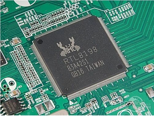
The RTL8198 is provided in a Thermally Enhanced Low Profile Plastic Quad Flat Package, 216-Lead (LQFP216-E-PAD) package. It requires only a 3.3V and 1.0V external power supply.
Features
SOC
Embedded RISC CPU, RLX5281 with 16K I-Cache, 8K D-Cache, 40K I-MEM, 8K D-MEM
Supports MIPS-1 ISA, MIPS16 ISA
Clock rate: 500MHz~620MHz
Provides a standard 5-signal P1149.1 EJTAG test port
Supports RLX5281 CPU suspend mode
L2 Capabilities
Six Gigabit Ethernet MACs switch with five IEEE 802.3 10/100/1000Mbps physical layer transceivers
Supports 1 dedicated GMII/RGMII/MII port to connect to an external MAC or PHY (supports both PHY mode and MAC mode) for HomePlug or HomePNA applications on RTL8198
Non-blocking wire-speed reception and transmission and non-head-of-line-blocking/forwarding
Internal 512Kbit SRAM for packet buffering
Internal 1024 entry 4-way hash L2 look-up table
Supports source and destination MAC address filtering
Three LED indicators per port for link, speed, full/half duplex
Bi-color LED display mode
CPU Interface (NIC)
Supports BSD mbuf-like packet structure with adjustable cluster size (128-byte to 2Kbyte) to provide optimum memory utilization
The NIC DMA support multiple-descriptor-ring architecture for QoS applications (supports 6 RX descriptor rings and 2 TX descriptor rings)
Peripheral Interfaces
Supports PCI Express Host with integrated PHY to connect up to two master devices
Two PCI Express PHY embedded
Supports one USB 2.0 host controller for access to USB-supported peripherals
One USB PHY is embedded
Supports two 16550 UARTs
Supports up to 44 GPIO pins
Memory Interfaces
Serial Flash (SPI Type)
Supports two banks and dual I/O channels for SPI Flash application
Each Flash bank could be configured as 256K/512K/1M/2M/4M/8M/16M Bytes
Boot up from SPI flash is supported
SDR DRAM
Supports two SDR DRAM banks; each can be configured as 2M/4M/8M/16M/32M/64Mbyte
16bit SDR DRAM data bus supported. System totally supports up to 128Mbyte SDR DRAM memory space
DDR1 DRAM
Supports one DDR1 DRAM bank that can be configured as 16M/32M/64M/128Mbytes
16-bit DDR1 DRAM data bus supported. System totally supports up to 128Mbyte DDR1 DRAM memory space
DDR2 DRAM
Supports one DDR2 DRAM bank that can be configured as 32M/64M/128Mbyte
16-bit DDR2 DRAM data bus supported. System totally supports up to 128Mbyte DDR2 DRAM memory space
Supports Green Ethernet
Cable length power saving
Power down power saving
Supports IEEE 802.3az Energy Efficient Ethernet ability for 1000Base-T, 100Base TX in full duplex operation and 10Base-T in full/half duplex mode
Other Add-on-Value Features
Supports Link Down Power Saving in Ethernet PHYceivers
Supports two hardware timers and one watchdog timer
Per-port configurable auto-crossover function
Built-in regulator controller
DDR1 DRAM to transform 3.3V to 2.5V via an external BJT transistor
DDR2 DRAM to transform 3.3V to 1.8V via an external BJT transistor
Supports Non-Flash Boot Interface (NFBI)
Single 25MHz crystal or 40MHz clock input
LQFP216-E-PAD package
相关产品推荐
-
 供应HT46R01C单片机,合泰小体积OTP单片机,8位单片机
-
 供应微芯单片机PIC16F723A-I/SS,全新13年深圳现货
-
 低成本3W,5W球泡灯驱动方案,SM7523B,SM7525灯杯驱动
-
 供应600V快恢复二极管MUR3060PTG,3A大电流快恢复管
-
 供应4A800V场效应管STD4NK80Z,LED驱动电源功率管
-
 仕兰代理,36V 1A驱动IC,SD42522大功率LED驱动芯片
-
 供应FPGA主控单片机EP1C6Q240C8,军用Cyclone系列
-
 供应100MA线性LDO,双路线性稳压器MAX8865TEUA
-
 供应5V2.1A三星车充方案
-
 供应STW20NK50Z大功率MOS管,500V场效应管深圳现货